Scalable spatiotemporal interleaving network for high-density integrated photonic convolution
可扩展的用于高密度集成光子卷积的时空交错网络
高密度統合光子畳み込みのためのスケーラブルな時空間インターリーブネットワーク
고밀도 통합 광학 컨볼루션을 위한 확장 가능한 시공간 인터리빙 네트워크
Red de entrelazamiento espacio-temporal escalable para convolución fotónica integrada de alta densidad
Réseau d'interlacement spatio-temporel scalaire pour la convolution photonique intégrée à haute densité
Масштабируемая пространственно-временная сеть переключения для высокоплотной интегрированной фотонной свертки
Hudi Liu 刘虎迪, Jingchi Li 李靖驰, Hua Zhong 钟华, Yu He 何宇, Yikai Su 苏翼凯
State Key Laboratory of Photonics and Communications, School of Integrated Circuits, Shanghai Jiao Tong University, Shanghai 200240, China
中国 上海 上海交通大学集成电路学院 光子传输与通信全国重点实验室
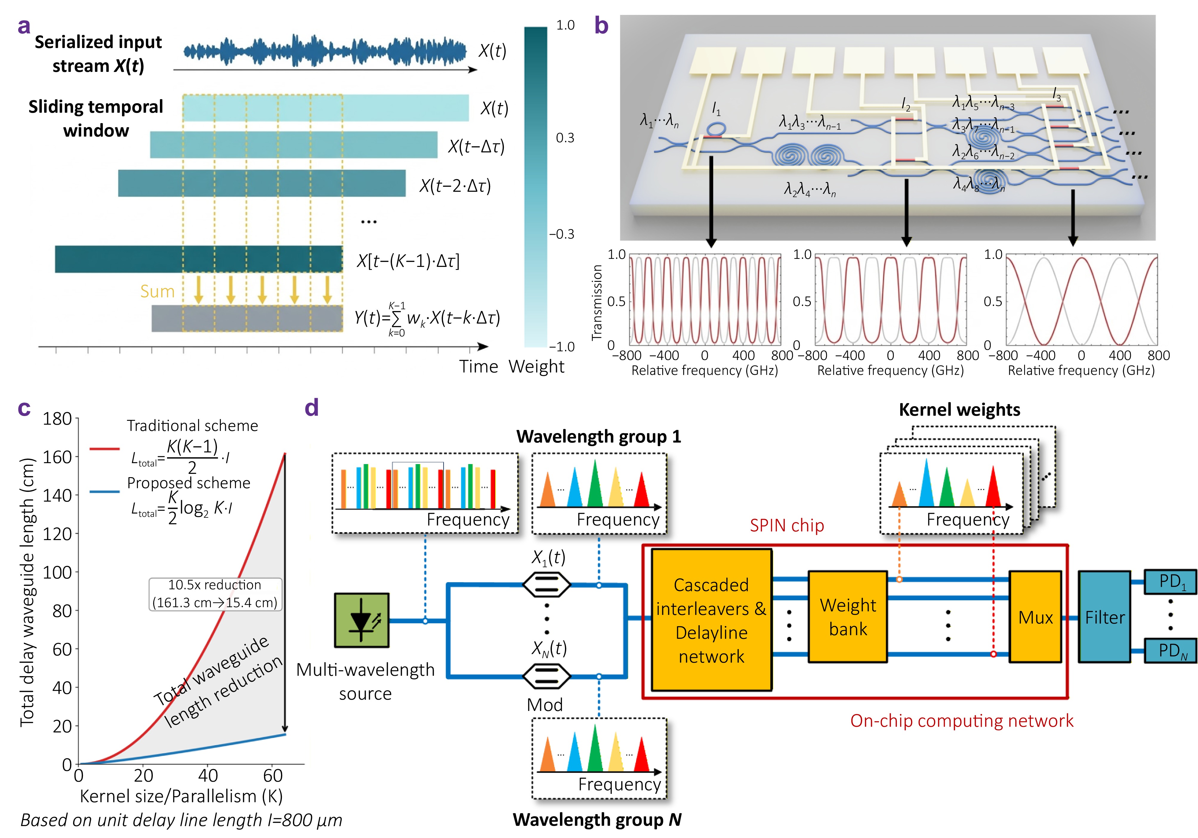
Efficient edge intelligence is fundamentally constrained by data movement overhead in conventional electronic hardware, motivating alternative computing paradigms with intrinsic parallelism. Although integrated photonic processors provide multiple parallel dimensions, established architectures remain limited by the quadratic scaling of both footprint and control complexity with rising computational throughput.
Here, we propose an on-chip spatiotemporal photonic interleaving network (SPIN) that enables convolutional acceleration by recursively interleaving distributed delay lines into shared physical channels, thereby redistributing throughput scaling from spatial replication to wavelength multiplexing while reducing waveguide footprint to O(K log2 K) and active control complexity to O(K). Experimental results demonstrate high-fidelity convolution with a correlation coefficient exceeding 0.98 on the Modified National Institute of Standards and Technology (MNIST) dataset, complemented by programmable multi-task operation and configurable kernel geometry.
The SPIN architecture is capable of supporting a projected single-core throughput of 29.7 TOPS upon full exploitation of the available spectrum. These results validate a structurally scalable and energy-efficient photonic computing framework, advancing the viability of integrated optical accelerators for next-generation edge AI.