High performance integrated photonic circuit based on inverse design method
基于逆向设计方法的高性能集成光子电路
逆解法による高性能光集積回路
역설계 방식에 기반한 고성능 집적 광자회로
Circuito fotónico integrado de alto rendimiento basado en el método de diseño inverso
Circuit photonique intégré haute performance basé sur la méthode de conception inverse
Высокопроизводительная интегральная фотонная схема, основанная на методе обратного проектирования
Huixin Qi 齐慧欣 ¹, Zhuochen Du 杜卓晨 ¹, Xiaoyong Hu 胡小永 ¹ ² ³, Jiayu Yang 杨佳宇 ¹, SaiSai Chu 褚赛赛 ¹, Qihuang Gong 龚旗煌 ¹ ² ³
¹ State Key Laboratory for Mesoscopic Physics & Department of Physics, Collaborative Innovation Center of Quantum Matter & Frontiers Science Center for Nano-optoelectronics, Beijing Academy of Quantum Information Sciences, Peking University, Beijing 100871, China
中国 北京 北京大学 人工微结构和介观物理国家重点实验室 量子物质科学协同创新中心 纳光电子前沿科学中心
² Peking University Yangtze Delta Institute of Optoelectronics, Nantong 226010, China
中国 南通 北京大学 长三角光电科学研究院
³ Collaborative Innovation Center of Extreme Optics, Shanxi University, Taiyuan 030006, China
中国 太原 山西省极端光学协同创新中心
The basic indexes of all-optical integrated photonic circuits include high-density integration, ultrafast response and ultra-low energy consumption. Traditional methods mainly adopt conventional micro/nano-structures. The overall size of the circuit is large, usually reaches hundreds of microns. Besides, it is difficult to balance the ultrafast response and ultra-low energy consumption problem, and the crosstalk between two traditional devices is difficult to overcome.
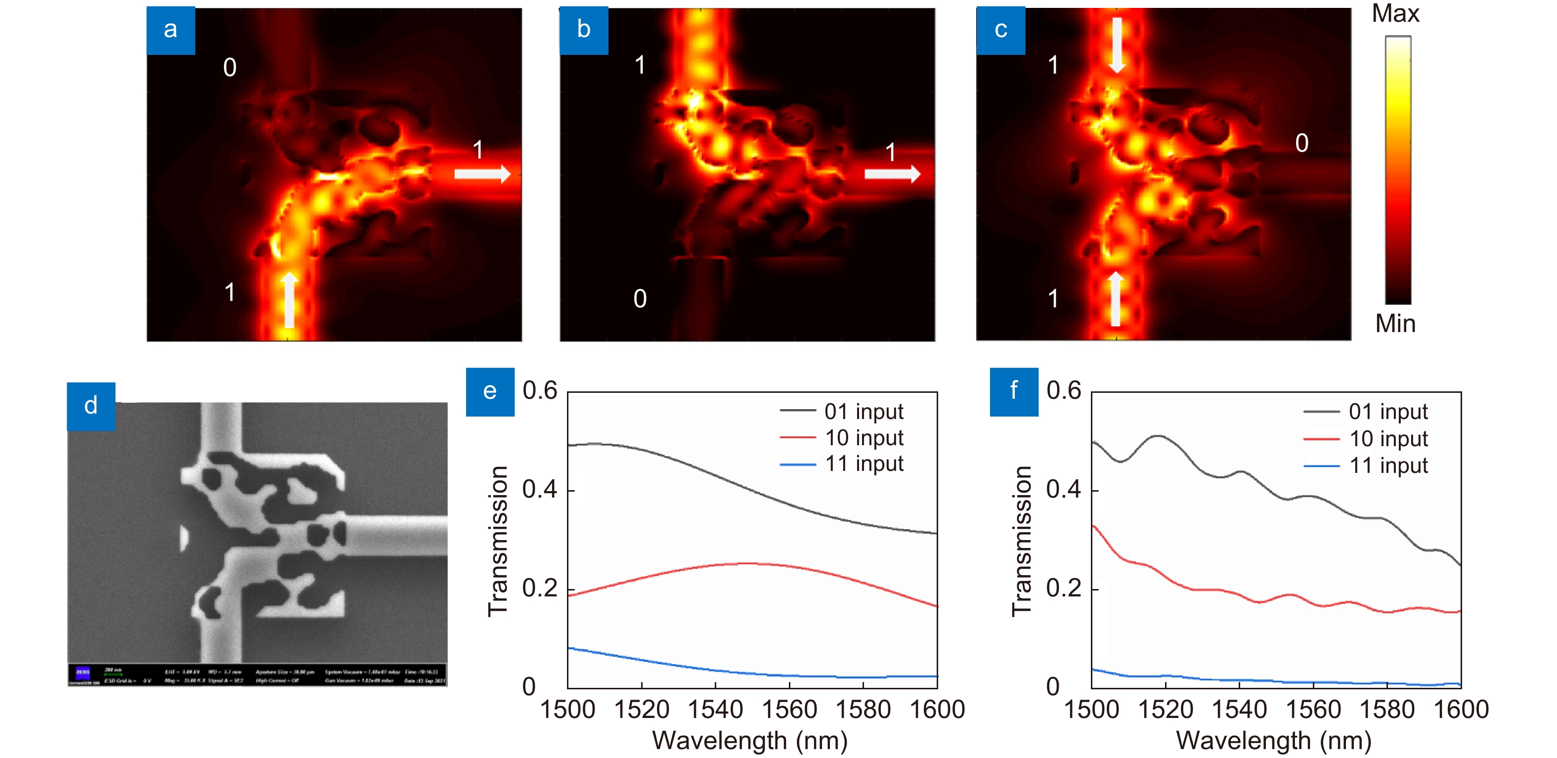
Here, we propose and experimentally demonstrate an approach based on inverse design method to realize a high-density, ultrafast and ultra-low energy consumption integrated photonic circuit with two all-optical switches controlling the input states of an all-optical XOR logic gate. The feature size of the whole circuit is only 2.5 μm × 7 μm, and that of a single device is 2 μm × 2 μm. The distance between two adjacent devices is as small as 1.5 μm, within wavelength magnitude scale. Theoretical response time of the circuit is 150 fs, and the threshold energy is within 10 fJ/bit.
We have also considered the crosstalk problem. The circuit also realizes a function of identifying two-digit logic signal results. Our work provides a new idea for the design of ultrafast, ultra-low energy consumption all-optical devices and the implementation of high-density photonic integrated circuits.