Ultrafast laser direct writing of highly conductive copper micropatterns
高导电铜微图案的超快激光直写
高導電性銅マイクロパターンの超高速レーザー直写
고전도성 구리 마이크로 패턴의 초빠른 레이저 직접 쓰기
Escritura directa láser ultrarápida de micropatrones de cobre altamente conductores
Écriture directe laser ultrarapide de micromotifs de cuivre hautement conducteurs
Ультрабыстрая лазерная прямая запись высокопроводящих медных микроузоров
Songyan Xue ¹, Chunsan Deng ¹, Mingduo Zhang ¹, Huace Hu ¹, Fayu Chen ¹, Leimin Deng ¹, Jianguo Liu ¹, Hui Gao ¹ ², Wei Xiong ¹ ²
¹ Wuhan National Laboratory for Optoelectronics, School of Optical and Electronic Information, Huazhong University of Science and Technology, Wuhan 430074, China
中国 武汉 华中科技大学光学与电子信息学院 武汉光电国家研究中心
² Optics Valley Laboratory, Hubei 430074, China
中国 武汉 湖北光谷实验室
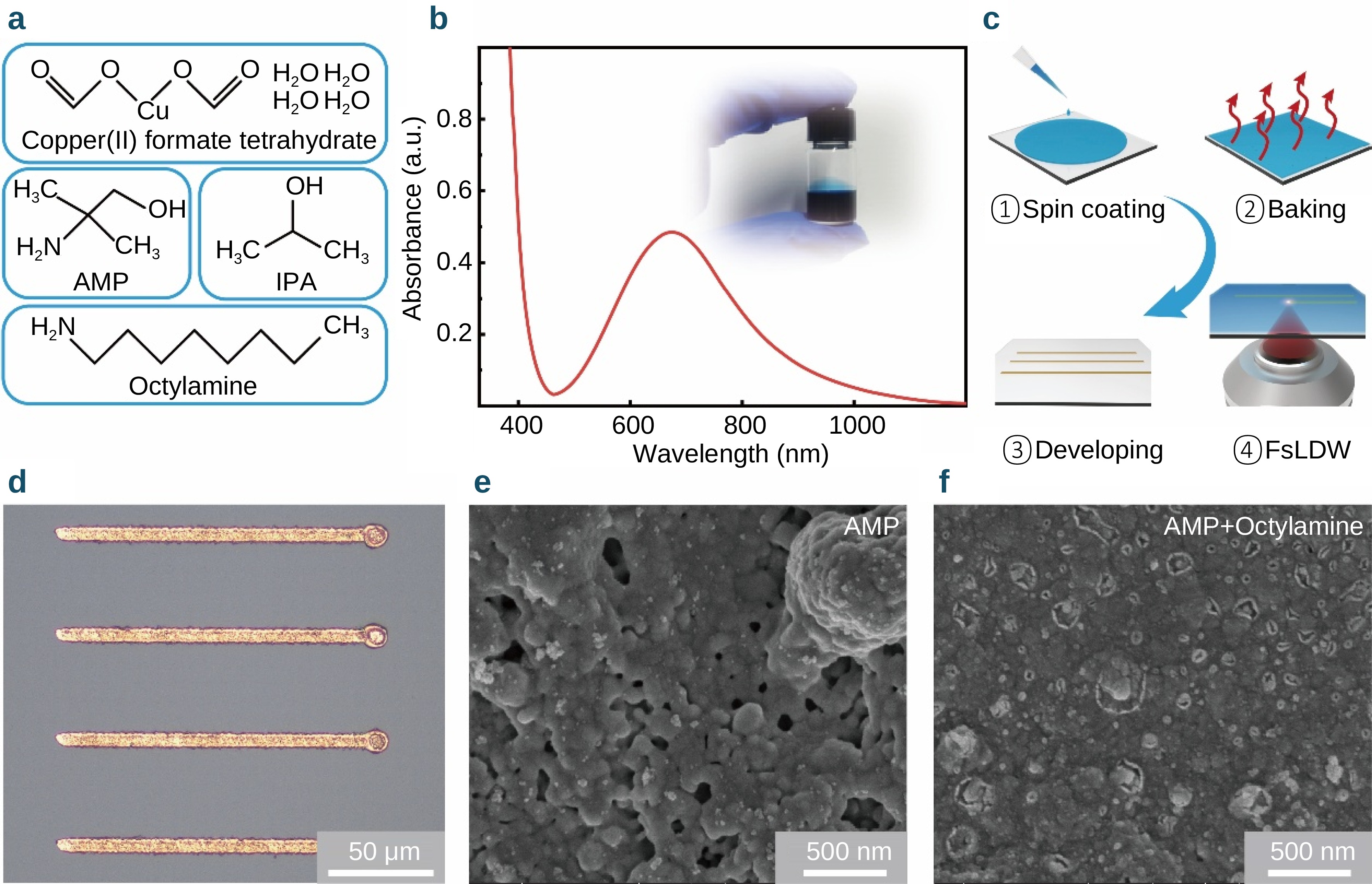
Copper (Cu) interconnects are fundamental to advanced optoelectronic systems. Femtosecond laser direct writing (FsLDW) employing particle-free Cu ion inks provides a compelling “cold processing” approach; however, it frequently results in porous, high-resistivity structures caused by disordered grain growth and solvent-induced micro-explosions.
Here, we report a high-precision FsLDW strategy utilizing a specifically formulated metal-organic complex ink. By decreasing the reduction energy barrier and regulating crystallization via a composite amine complex, combined with a pre-baking step to suppress micro-explosions, we achieve Cu micropatterns with a highly dense surface morphology under ambient conditions. The resulting structures demonstrate a minimum resistivity of 9.34 μΩ·cm (approximately 5.5 times that of bulk Cu) while maintaining sub-10 μm linewidths.
Moreover, this method exhibits broad processing adaptability and substrate compatibility, facilitating reliable metallization on flexible substrates, macroscopic wafers, and curved surfaces. The fabricated Cu interconnects function as stable signal and power transmission pathways within a fully FsLDW-patterned UV photodetector. This study establishes a practical route for deploying high-performance conductive networks in advanced electronic systems.