Optical packaging of photonic integrated circuits: bottlenecks and potential solutions
光子集成电路的光学封装:瓶颈和潜在解决方案
フォトン集積回路の光パッケージ:ボトルネックと潜在的ソリューション
광자 통합회로의 광학 포장: 병목과 잠재적 인 솔루션
Embalaje óptico de circuitos integrados fotonicos: cuellos de botella y soluciones potenciales
Emballage optique des circuits intégrés photoniques : goulets d’étranglement et solutions potentielles
Оптическая упаковка фотонных интегральных схем: узкие места и потенциальные решения
Rodrigo Rendeiro ¹ ², Hugo Neto ², Diogo Vaz ², Carla Rodrigues ², Heming Wei ³, Jan Nedoma ⁴, Antonio Teixeira ² ⁵, Francisco Rodrigues ², Carlos Marques ¹ ⁶
¹ CICECO-Aveiro Institute of Materials & Physics Department, University of Aveiro, Aveiro 3810-193, Portugal
² PICadvanced S.A., PCI-Creative Science Park Via do Conhecimento, Edifício Central, Ílhavo 3830-352, Portugal
³ Key Laboratory of Specialty Fiber Optics and Optical Access Networks, Joint International Research Laboratory of Specialty Fiber Optics and Advanced Communication, Shanghai University, Shanghai 200444, China
中国 上海 上海大学特种光纤与先进通信国际合作联合实验室 特种光纤与光接入网重点实验室
⁴ Department of Telecommunications, VSB-Technical University of Ostrava, Ostrava 70800, Czech Republic
⁵ IT-Instituto de Telecomunicações, Campus Universitário De Santiago, Aveiro 3810-193 , Portugal
⁶ Department of Physics, VSB-Technical University of Ostrava, Ostrava 70800, Czech Republic
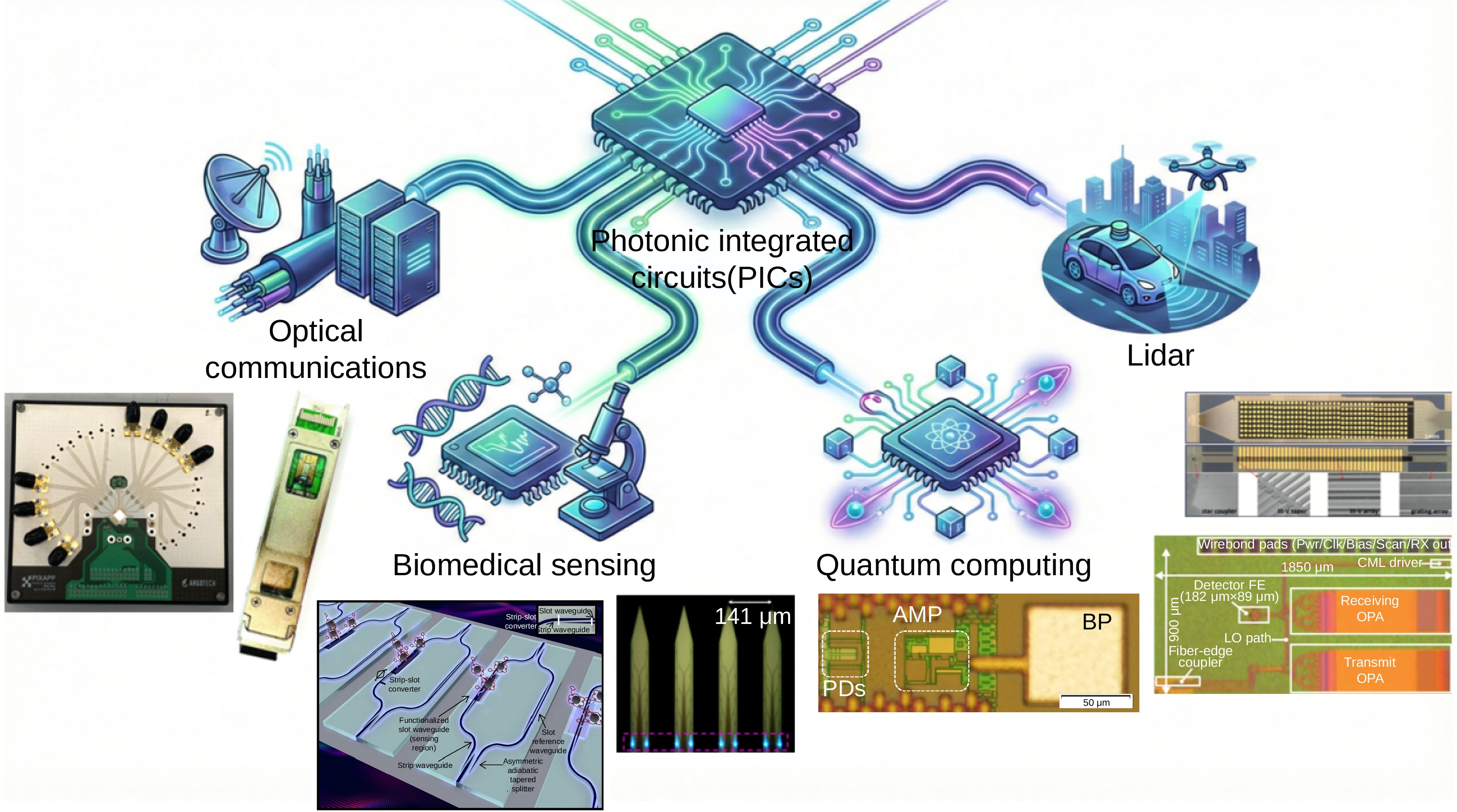
Photonic integrated circuits (PICs) are revolutionizing telecommunications, quantum computing, and sensing applications by manipulating light instead of electrical signals, bringing unprecedented improvements in speed, bandwidth, efficiency and integration density.
However, optical packaging remains a critical bottleneck for mass deployment of PIC-based products and components, primarily due to mode field diameter (MFD) mismatch between fibers and PIC waveguides and its sub-micron alignment tolerances, hindering efficient optical coupling, as well as rapid and reproducible PIC assembly processes. Key challenges also include thermal management through coefficient of thermal expansion (CTE) matching, optical adhesive selection, and standardized design rules for scalable packaging.
This paper reviews current optical coupling approaches, comparing surface and edge coupling methods, while evaluating emerging solutions including two-photon polymerization (TPP) for 3D micro-optical structures and self-written waveguides (SWWs) with self-aligning capabilities. Novel alignment strategies, from active feedback systems to AI-driven algorithms and passive techniques are also investigated.
Future prospects highlight inverse-designed structures, silicon nitride integration for high-power applications and nanoimprint lithography for mass production, paving the way for wafer-level optical packaging solutions.